Description
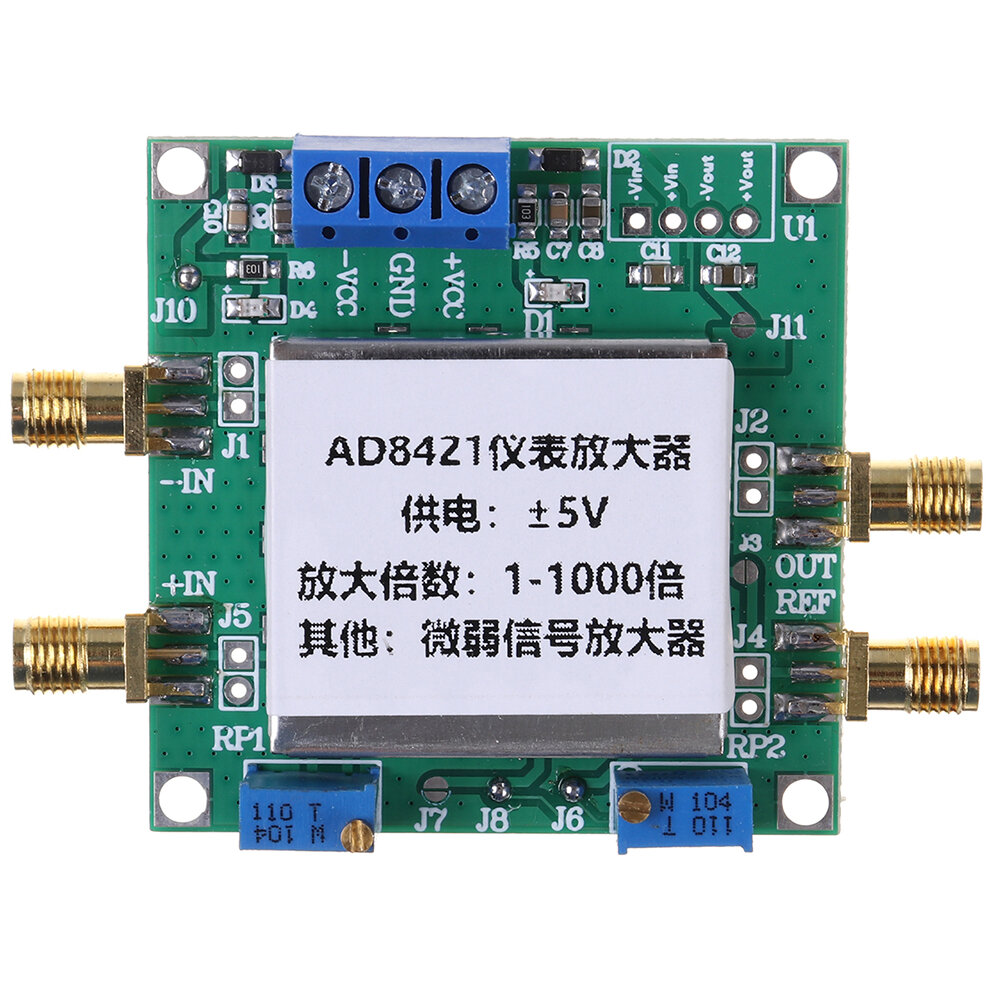
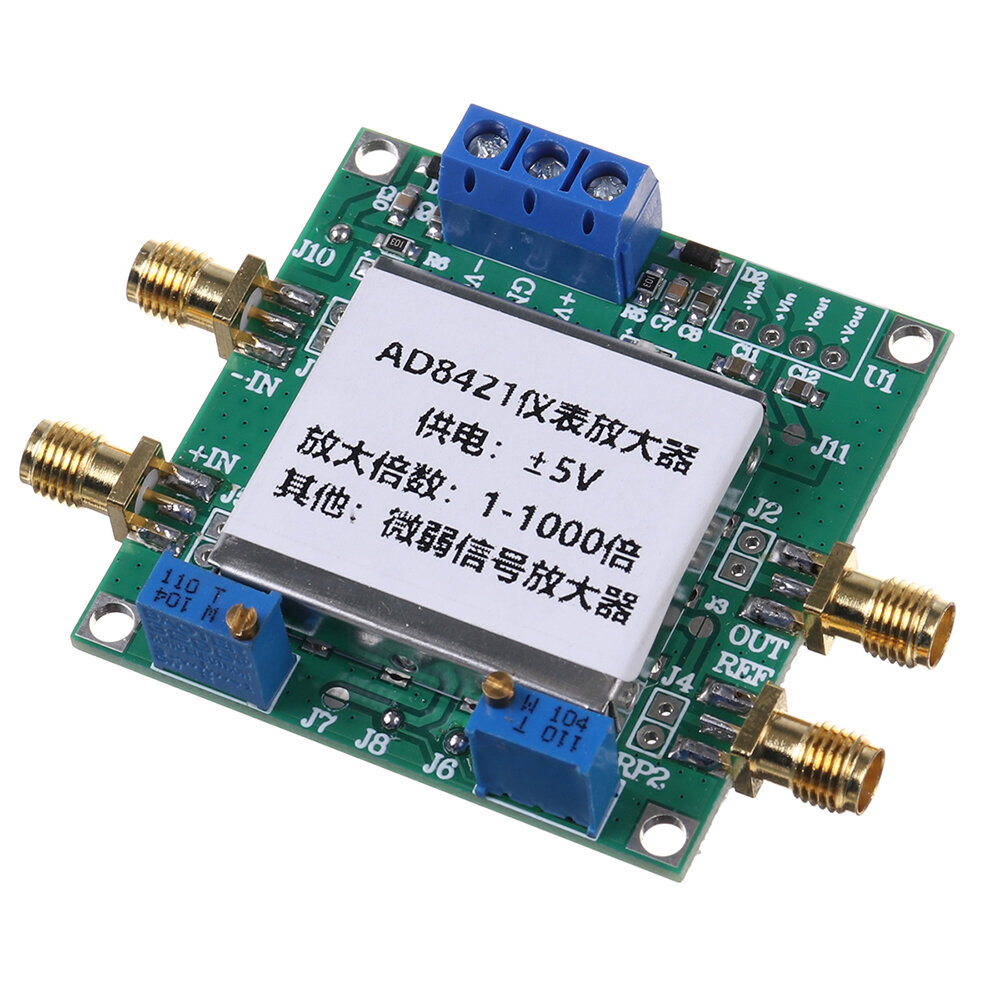
Description:AD8421 is a high-speed instrumentation amplifier with low cost, low power consumption, extremely low noise, and ultra-low bias current. It is especially suitable for various signal conditioning and data acquisition applications. This product has a very high common-mode rejection ratio (CMRR), which can extract low-level signals submerged in high-frequency common-mode noise in a wide temperature range.
The AD8421 has a bandwidth of 10 MHz, a slew rate of 35 V/µs, and a settling time of 0.001% (G = 10) of 0.6 µs. It is capable of amplifying high-speed signals and is outstanding in applications requiring high-channel-count multiplexing systems. Even in the case of high gain, the current feedback architecture can ensure high performance. For example, when G = 100, the bandwidth is 2 MHz and the settling time is 0.8 µs. AD8421 has excellent distortion performance and is suitable for demanding applications such as vibration analysis.
AD8421 provides 3 nV/?Hz input voltage noise and 200 fA/?Hz current noise performance, and the quiescent current is only 2 mA, which is very suitable for measuring low-level signals. For applications with larger source impedances, the AD8421 uses innovative process technology to provide noise performance limited only by the sensor.
AD8421 uses a unique protection method to ensure robust input while maintaining extremely low noise. With this protection function, even if the difference between the input voltage and the opposite power rail reaches 40 V, it will not cause damage.
The gain can be set from 1 to 10,000 through a resistor. The reference pin can be used to apply a precise offset to the output voltage.
The AD8421 has a rated operating temperature range of ?40°C to +85°C and can guarantee typical performance curves up to 125°C. It is available in 8-pin MSOP and SOIC packages.
Specification:
Product size: 50 x 50 x 9mmProduct weight: 20g1. Low power consumption: the maximum power supply current is 2.3 mA.2. Low noise:The maximum input voltage noise at 1 kHz is 3.2 nV/?Hz;Current noise at 1 kHz: 200 fA/?Hz (at 1 kHz).3. Excellent communication characteristics:Bandwidth: 10 MHz (G = 1);Bandwidth: 2 MHz (G = 100);0.001% settling time: 0.6 µs (G = 10);Common mode rejection ratio (CMRR): 80 dB (20 kHz, G = 1).35 V/µs slew rate4. High precision DC performance (AD8421BRZ)CMRR: 94 dB (minimum value, G = 1)Input offset voltage drift: 0.2 µV/°C (maximum)Maximum gain drift: 1 ppm/°C (G = 1)Input bias current: 500 pA (maximum)5. Wide power supply range: 5V to 36 V single power supply; dual power supply: ±2.5 V to ±18 V.6. Input overvoltage protection: Input overvoltage protection can exceed 40V of reverse power supply7. Gain: The gain is set by a single resistor (G = 1 to 10,00)Default delivery: 10 times gain, you can adjust the gain through the potentiometer.
Schematic description:
1. Adopt single power supply mode:
If the input signals (IN- IN+) are within the range of 0~VCC positive power supply (including differential signals with DC bias), the module only needs a single power supply. At this time, disconnect J10, J11; connect J7, J8, J6, the module is working in a single power supply state at this time, and the DC bias voltage can be input from the SMA3 (or J4) end (or J6 is connected, and the bias voltage is set by the potentiometer).
2. Adopt dual power supply mode:
The input voltage is dual power supply, the default delivery: disconnect J7, J11; connect J10, J8The input voltage is a single power supply and requires negative voltage module conversion. The default delivery: disconnect J5; connect J10, J11, J8, J6If the input signal (IN- IN+) contains negative voltage components or pure AC signals, the module needs dual power supply. At this time, turn off J7; turn on J8, J10, J11, and the module is working in dual power state. SMA3 (or J4) terminal input DC bias voltage, (or turn on J7, the bias voltage is set by the potentiometer).Output signal Vout=[(Vin+)-(Vin-)]*G+VrefG = 1 + (9.9 k?/RG)
Package included:
1 x AD8421 amplifier module


