Description
Product Features:Ultra-high-speed slew rate: 5500 V/?s (4 V step, G = +2) Rise time: 545 ps (2 V step, G = +2) large signal bandwidth 440 MHz, G = +2 320 MHz, G = +10 Small signal bandwidth (3 dB) 1 GHz, G = +1 700 MHz, G = +2 0.1% Settling time: 10 ns (2 V step, G = +2) Low in wide bandwidth Distortion spurious-free dynamic range (SFDR) 66 dBc (20 MHz, second harmonic) 75 dBc (20 MHz, third harmonic) Third-order intercept point (3IP) 26 dBm (70 MHz, G = + 10) Good video specification 0.1 dB gain flatness up to 75 MHz 0.01% differential gain error, RL = 150 ? 0.01° differential phase error, RL = 150 ? high output drive 175 mA output load drive current 10 dBm and SFDR is 38 dBc(70 MHz, G = +10) Power supply Power supply voltage: +5 V to ±5 V Power supply current: 14 mA (typical value) Application pulse amplifier Intermediate frequency/RF gain stage/Amplifier High-resolution video graphics High-speed instrumentation CCD Imaging amplifier
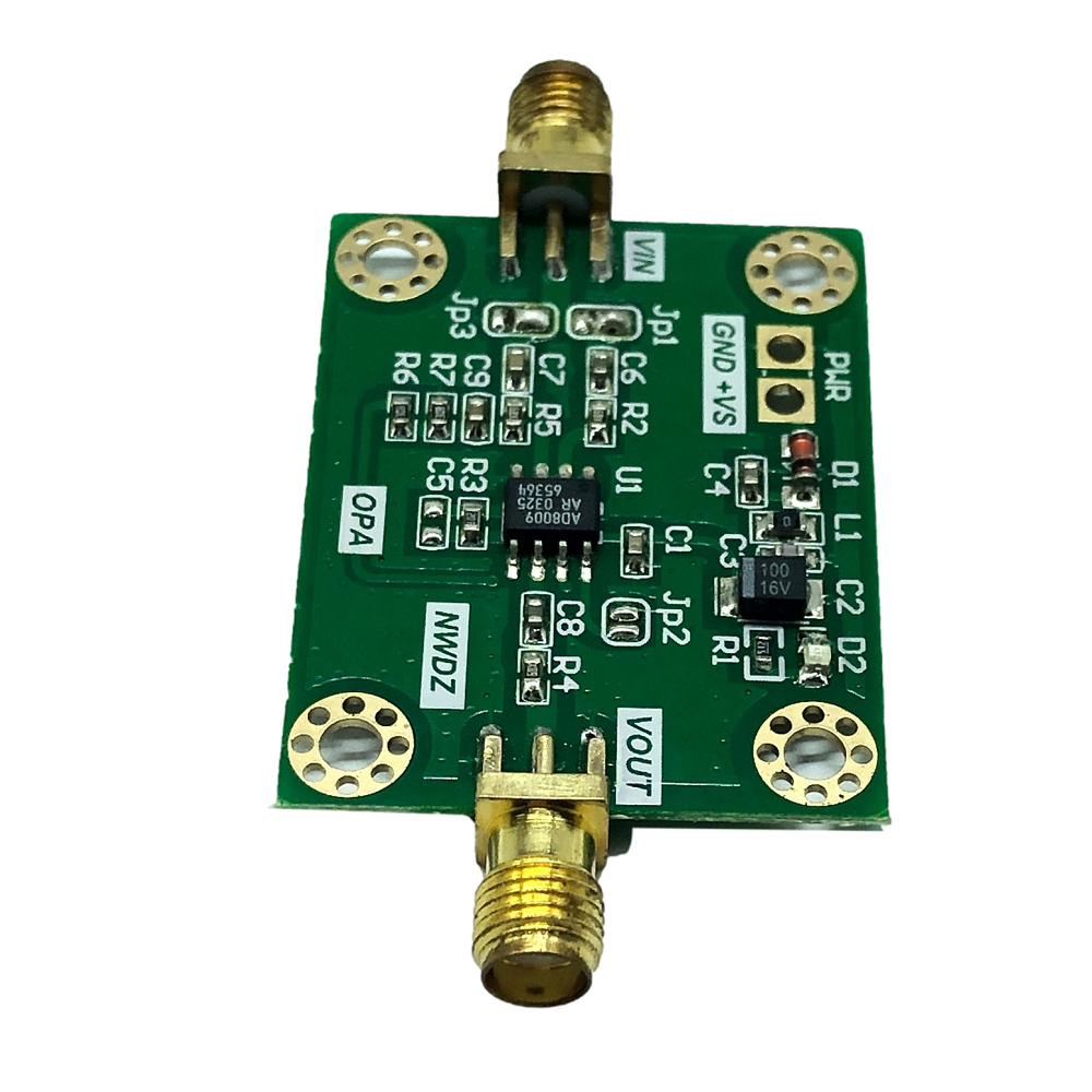
1. Single power supply 6~12V anti-reverse connection protection2. UHV slew rate can be used for pulse amplification, square wave amplification, etc.3. High output current 175mA4. The default input and output impedance is 50R, and the default gain of in-phase amplification is 5 times.6. Provide schematic diagrams and related information
Package included:
1 x AD8009 Module
Operational amplifier terminology:
Common Mode Voltage Range (CMVR)Also called the input voltage range, CMVR is the allowable input voltage range of the two input terminals. If it exceeds this range, the output will have clipping or excessive nonlinearity.
Common Mode Rejection Ratio (CMRR)The ratio of the common-mode voltage range (CMVR) to the input offset voltage (?VoOS) change in this range, and the result is expressed in dB. CMRR (dB) = 20log (CMVR/?VOS)
Full power bandwidthRefers to the maximum frequency measured at unity gain. At this frequency, the rated output voltage of a sinusoidal signal can be obtained on the rated load, and the slew rate limit will not cause distortion.
Gain bandwidth product (GBW)The product of open-loop gain and bandwidth at a specific frequency.
Input bias current (IB)The current of the input pin.
Input bias current driftThe proportional change of the input bias current with respect to the temperature within the rated temperature range.
Input offset currentThe difference between the two input currents.
Input offset current driftsThe rate of change of the input offset current within the rated temperature range when the output maintains a constant voltage.
Input offset voltage drifts (TCVOS)The ratio of the input offset voltage change to the temperature change.
Offset voltage (VOS)To obtain zero output voltage, the required differential voltage at the input pins of the op amp. The range of offset voltage varies depending on the process and design technology: Auto-zero operational amplifier: <1 ?V Precision operational amplifier: 50 ?V to 500 ?V Best bipolar operational amplifier: 10 ?V to 25 ?V Best JFET Input operational amplifier: 100 ?V to 1000 ?V Best bipolar high-speed operational amplifier: 100 ?V to 2000 ?V Unadjusted CMOS operational amplifier: >2 mV DigiTrim® CMOS operational amplifier: <100 ?V to 1000 ?V
Open loop gain (AVO)The ratio of the output voltage to the input offset voltage between the two input pins. The result is expressed in dB. Usually only the gain at DC (AO) is specified, but for many applications, such as high-speed amplifiers used in video and RF, the frequency dependence of the gain is also very important. Based on this, we give the open loop gain and phase response of each amplifier.
Operating power supply voltage rangeThe range of power supply voltage that can be applied to the amplifier when the amplifier is operating within the rated range. Operational amplifier circuits for many applications use balanced dual power supplies, but some applications use single power supplies for energy saving or other reasons. For example, battery power supplies in automobile and ship equipment provide only one polarity. Even line-powered devices, such as computers, may have only unipolar power supplies, providing the system with +5 V or +12 V DC power, or as low as 1.8 V, and newer applications use even lower voltages.
Power Supply Rejection Ratio (PSRR)The ratio of the change in the supply voltage to the change in the input offset voltage, and the result is expressed in dB. PSRR = 20log (?VSY/?VOS)
Establishment timeAfter a step input is applied, the time required for the amplifier to settle to a predetermined accuracy level or percentage of output voltage.
Slew rateUnder large signal conditions, the maximum rate of output voltage change, the result is usually expressed in V/?s.
Power supply currentThe current that the power supply voltage needs to provide when the amplifier is working under no load.
Small signal unity gain frequencyThe frequency at which the open loop gain is 1 or 0 dB. Only applicable to signals below 200 mV. Due to the slew rate limitation, a large output voltage swing cannot be obtained at high frequencies.


